In this tutorial, we will be discussing about the basics of mosfets, types and their use in robotic applications.
INTRODUCTION:
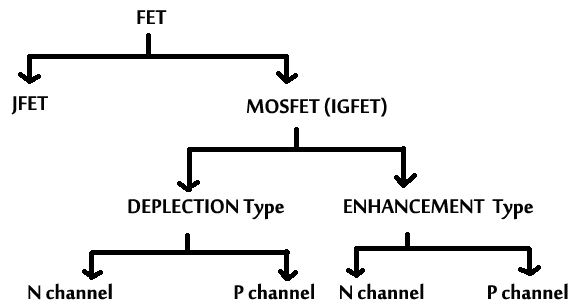
A MOSFET (Metal oxide semiconductor field effect transistor) is basically a transistor and in particular it is a FET as shown in the figure below.
https://analogelectronicshelp.files.wordpress.com/
It is basically a four terminal device consisting of a gate, source, drain and a body. There are two types of MOSFETs. One is Enhancement mode and the other is Depletion mode.
DESIGN (STRUCTURE):
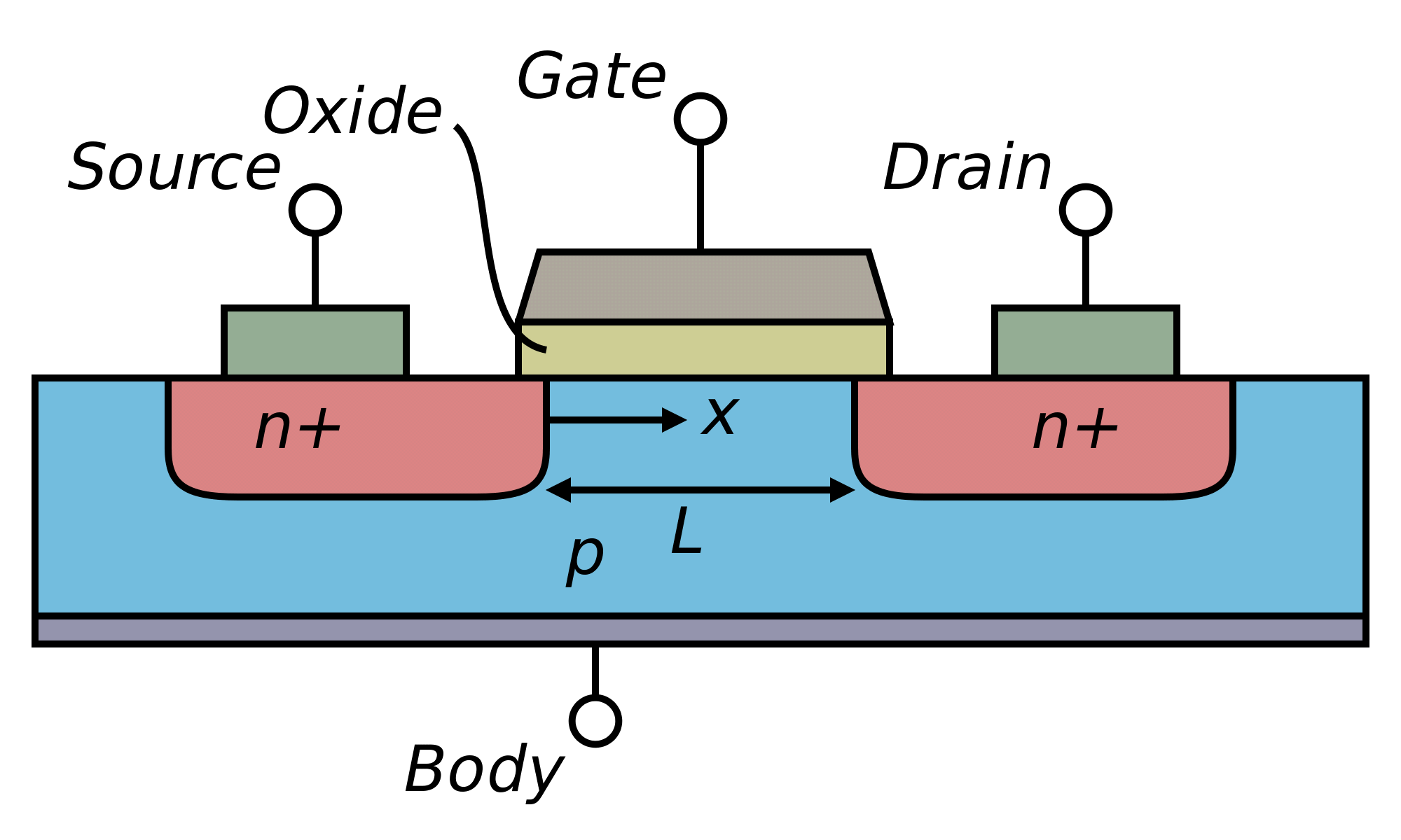
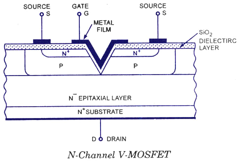
When we come to the design of N-Channel MOSFET, it actually has a P-type body in which an N-type source
and an N-type drain are diffused. On the body an insulated SiO2 layer is present. On the above, a layer insulates
a metallic layer exists and this metallic layer is the gate. Thus the gate is always isolated from the body. This is
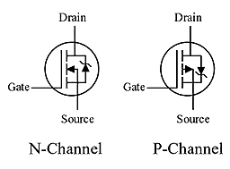
the main difference between a FET and a MOSFET in design. You can see this in below figure-3.P-channel
MOSFET is just a reverse of the N-channel MOSFET.
http://electronics.stackexchange.com/
https://en.wikipedia.org
We have known the design of the MOSFET. Now we will go through the applications of the device. It is mainly used for amplifying and switching signals.
WORKING:
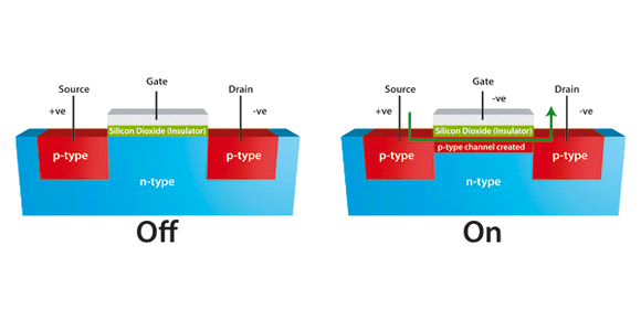
The metallic gate and body of the MOSFET constitute as a capacitor and the SiO2 layer between them acts as a dielectric of the capacitor. This is called as the Gate Capacitance. As in capacitance, when one plate of the capacitor is given a positive charge the same amount of opposite charge gets induced on the other plate. So, in an N-channel MOSFET when a 5V is given to a gate (source is grounded) and as gate acts as one side of the capacitor it induces a negative charge in the body which acts as a second side of capacitor. Now the two N-type layers (drain and the source) conduct because a layer of negative charge is formed in the body and thus the negative charged electrons conduct between drain and source. When the drain is given a positive voltage, the electrons flow from source to drain. Thus, source means the source of electrons and the drain means the drain of electrons. When gate is kept at zero volts no induced negative charge is produced on the body and thus conduction doesn’t occur. Similarly in a P-channel when gate is given negative voltage holes conduct from drain to source and the MOSFET is said to be in ON condition and when no voltage is given the MOSFET doesn’t conduct and is said to be in OFF condition.
https://chipghost.wordpress.com/2014/03/11/sand-to-chip/
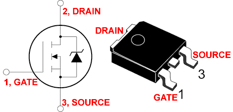
The early mosfets had a tendency to switch ON whenever high rise of drain to source voltage has occurred (high dv/dt).This resulted in catastrophic failures. This is due to the inherent transistor that is present in the MOSFET structure. If we observe carefully the above figure we can figure it out. For an N-channel MOSFET NPN transistor is present and for a P-channel MOSFET PNP transistor is present. So to avoid this thing both the source and the body are shorted through a process called source metallization. It is nothing but a metallic layer is used to short the source and body.When we see deeply into the working of MOSFET only the electrons or holes are used for conduction. Thus it is a mono-polar device unlike a BJT which is a bipolar device. MOSFETs have a high input resistance because of the SiO2 layer present in between the Gate and the body. Thus MOSFET takes very less current as input compared to a BJT to switch ON.Now we have known the design and the working of a MOSFET. I would like to tell you about how MOSFETs are being used in robotic applications.In robotics mosfets are mainly used in switching purposes like in changing the direction of a motor. For that we have to switch the MOSFET s, which is nothing but ON and OFF the mosfets. We know that the mosfets have some capacitance. So when a MOSFET is in ON position then the capacitor will be in the state of charging and when it is in OFF position the capacitor will be in discharging condition for a while. So for that purpose we will be connecting a resistor across the gate and the source in any circuit to discharge the capacitor. So, when a microcontroller pin is made high and given to a N-channel MOSFET then the MOSFET turns ON and a large amount of current flows across the drain and source. Thus we are controlling a huge amount of current across drain and source by giving very small current to gate.
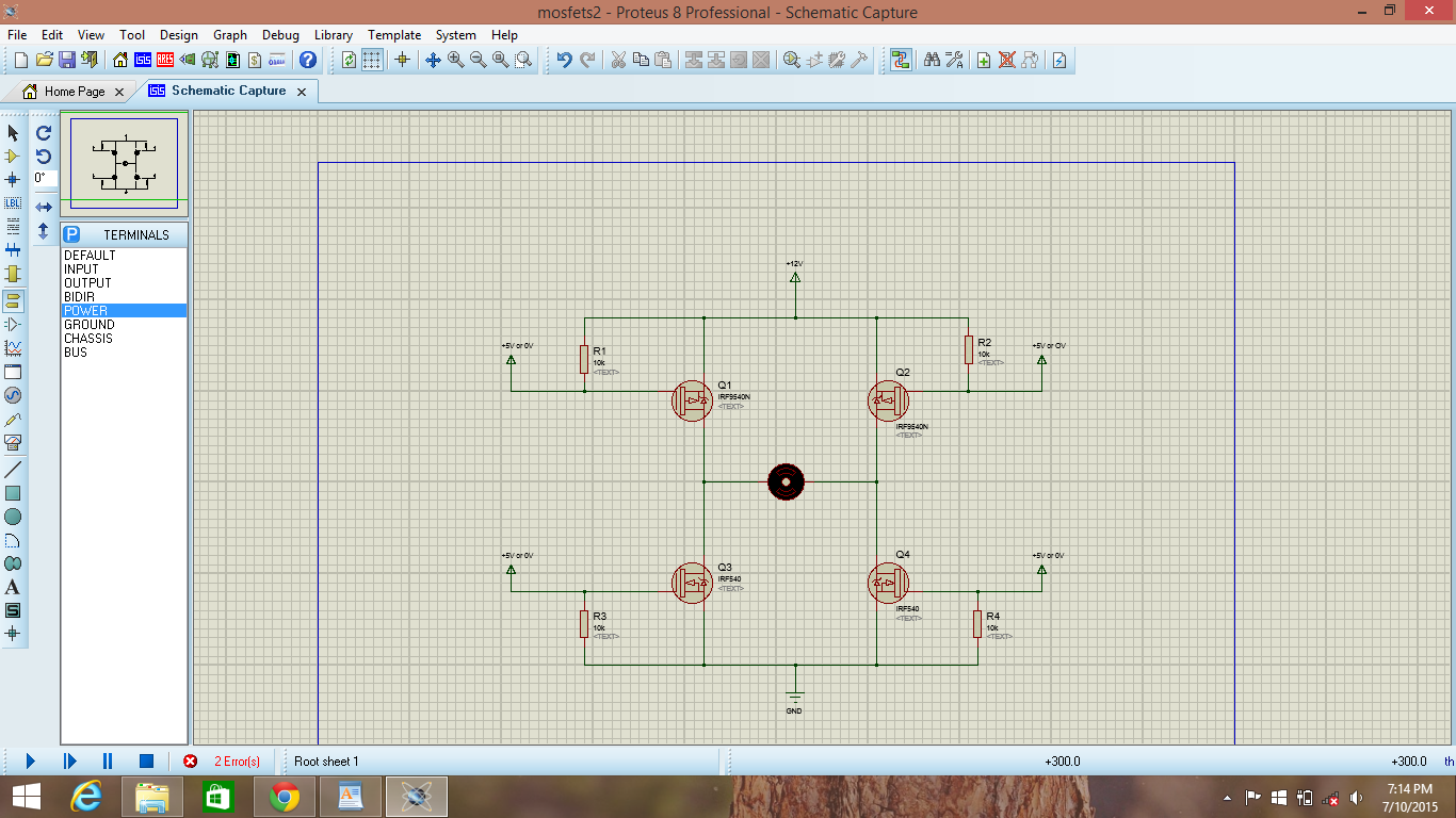
As of now we are comfortable with the basics of mosfets and how it acts as a switch. I would like to discuss about the H-Bridge that is used for controlling a motor. The fig3 consists of 4Mosfets Q1, Q2 ,Q3, Q4.All these 4 MOSFETS act nothing but like a switch. Q1 and Q2 are P-Channel mosfets and Q3 and Q4 are N-channel mosfets. In the below figure the two N-channel mosfets used are IRF-540 and the two P-channel mosfets used are IRF-9540.So, when Q1 and Q4 are in ON position then the motor moves in one direction and when the Q2 and Q3 are in one direction the motor moves in other direction. The figure, given below, is a circuit made in Proteus (simulation software). Don’t forget to connect the resistors to the 4 mosfets between gate and source. Thus now we can control a motor with the help of MOSFETs. Don’t switch ON both Q1 and Q3 or Q2 and Q4 together, if you do that then VCC and GND will get shorted and the MOSFETs will burn away. Don’t forget to put heat sinks for each and every MOSFET you use because during switching a huge amount of power loss occurs in the device which heats up the device easily. In that figure you can give either a +5V or 0V the gate as specified above to run the motor.
But this method is not so effective because the motor has some resistance and as high current flows through the circuit, there will be considerable voltage drop across the motor. So applying +5V at the gate cannot completely turn on the MOSFETs because now the source is not grounded. If a MOSFET is not completely turned on it cannot act like a short circuit as it will have some resistance, so it dissipates a large amount of power which is not considered as a good design. In such a case, a higher voltage to the gate is required, which cannot be given by the microcontroller itself. So we have to amplify the signal.This is the place where we need the use of a gate driver.A GATE DRIVER is generally an IC which is used in the design of a motor driver circuit to rectify the limitations that are caused due to the use of a MOSFET. Generally we will be using a power MOSFET for the motor driver circuit. The power mosfets have a larger capacitance compared to normal mosfets. So MOSFET driver is used to drive the high gate capacitance. While switching off the MOSFETs we know that the charging and discharging of capacitor occurs, so current should discharge from the capacitor in its OFF condition and it has to charge the
capacitor in ON position. So sometimes huge current spikes of 1A may be created while fast switching. So, to handle that currents we will be using gate or the MOSFET drivers.
The main disadvantage of MOSFETs is high resistance channels due to which a huge loss of power occurs in the MOSFETs and they start burning. One way to reduce this effect is by increasing the width of the MOSFET channels but this will greatly increase the cost of the MOSFETs.
POWER MOSFET:
By now, I hope that you understood the working of MOSFETs in turning a motor. Actually the MOSFETs, used in H-bridge circuit, are the power MOSFETs because as we all know that motor draws a large power and normal MOSFETs fail to sustain that much of high power. The design of power MOSFETs was made possible by the evolution of CMOS technology. CMOS (Complementary MOS) is nothing but the combination of the P-channel and the N -channel mosfets. The name suggests that the power MOSFETs are used to sustain high power conditions. We discussed in disadvantages section of MOSFETs that they have high channel resistance. This error is rectified in the design of power MOSFETs. A new type of VMOS technology evolved in the market.Designers started making vertical mosfets which have a less channel resistance. So many MOSFETs came into existence like Vertical diffused MOS, V-Groove and U-Groove etc. As the channel resistance gets reduced there will not be much power loss in the circuit due to MOSFETs.
You might have got confused between the input resistance (Gate resistance) and the channel resistance. Well, if it is so I will clear it to you now. The gate resistance is the resistance between the gate and the source which is caused due to the insulating SiO2 layer. For a good MOSFET this resistance should be high. Channel resistance is the resistance between the drain and the source channel and this has to be very less. Generally completely saturated mosfets have zero channel resistance, but when a MOSFET is not completely turned ON, then it has some resistance due to which a large power loss occurs in the H-Bridge type of circuits because the handling current is very high. This is the reason why channel resistance has to be less.
TESTING OF MOSFETS:
How do we test MOSFET? It’s actually pretty simple.Take a bread board, Multimeter and a 1K resistor (not necessarily 1K, just to make sure that the discharge of capacitor occurs). We know that when we give a +5V signal to gate and ground the source and give +5V to drain in a N-channel MOSFET the electrons flow from source to drain and the drain and source get shorted. So, when you keep Multimeter in continuity mode and test it, a beep sound occurs. You can refer to the circuit given below.
For a P-channel MOSFET, we know that when we give -5V to gate, +5V to source and ground the drain, then the source and drain get shorted and holes flow from source to drain. Thus when we keep DMM in continuity mode and check the continuity a beep sound occurs saying that the MOSFET is working fine. Here the source is the source of electrons and drain is the drain of electrons.