A normal human spends about 3 hrs/day in looking at photos in facebook,instagram.Have you ever wondered what happens in between the click in camera and the photo to be visible on your screen?
This tutorial gives a brief overview of
- History of cameras
- Basic structure of a camera(analog and digital are more or less alike)
- Electronics involved
- Terms used in camera technology and its effects on photos
HISTORY
Advances in technology are brought out rapidly during wars and also during space launches. Hasselblad 500 EL was carried by Neil Armstrong and Buzz Aldrin. The camera captured some astonishing images of mankind, first ever moon landing.
The Charge Coupled Device(CCD) was invented in 1969 at AT&T Bell Labs by Willard Boyle and George E. Smith. The CCD can be used to transfer charge along semiconductor device from one storage capacitor to other. The concept used was similar to Bucket Brigade Device which was developed in late 1960s. Initially CCDs were used as shift registers. In 1972, CCDs were patented for use in imaging.
BASIC STRUCTURE OF CAMERA
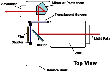
Fig:Top view of Camera
Source:electronics.howstuffworks.com
ELECTRONICS INVOLVED
Before going into the electronics,we need to know the definition of imaging as the entire camera is about making this imaging, simply images/photos.
Imaging is defined as “the conversion of optical scene(perceived by eyes) into electrical signal using a transducer.”
So,now we need an element which takes optical scene as input and gives electrical signal as output.Optical scene physically means light/photons as every object that we perceive through our eyes is characterised by photon energy.
So,we require an element which takes in photons and gives out voltage.
Photon → Voltage
Basic principle in physics states that “When a photon of particular wavelength(which corresponds to particular energy) is focused on a semiconductor,electrons excite from valence band to conduction band if the energy supplied is greater than band gap.”
For Si, which is the most used semiconductor, the band gap is about 1.12eV.
So,if there were photons from an object which is able to push electrons from valence band to conduction band,we are getting an information related to intensity of the object which can be extrapolated to get its digital representation.
Thus we are converting photonic energy into electrical energy which is the basic principle used in camera.
Finally our task is to
Photon → Charge → Electrical Voltage
PN junction semiconductor can be used for this one.It can be used in one of the two modes
- Forward bias
- Reverse bias
So,in which bias it can fulfill our purpose.Let’s take forward bias and proceed.
In forward bias,there is no depletion layer which indicates if a photon is projected on the semiconductor,it produces and electron-hole pair but this particular pair cannot be distinguished from others(as it is forward bias,it is in conduction mode and there will be many such pairs) So, this bias does not differentiate each and every pixel thus failing the basic purpose of camera.
A pn junction in reverse bias when incident by photons, the energy of photons is used to create electron-hole pair which are distinguishable(as they are rare).These electrons get accumulated in depletion capacitor/junction capacitor which converts it into electrical voltage. For different photon energies (different intensities of light) different levels of charges are produced in turn different electrical voltages are produced. These levels of voltages are used to identify the intensity of light incident. These semiconductors placed in an array are called pixels. Ever wondered what does MegaPixel of your phone camera signify? It is the number of pixels present in your phone camera sensor. For example a 4 MegaPixels camera has 2592 x 1520 pixels array.
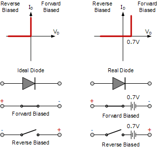
Fig:Forward and reverse bias of diode

Fig:Working of Photodiode
Source:Elprocus
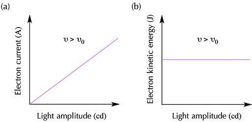
Fig:Graph of Light intensity vs current
DEEP INTO PIXELS
![]()
Fig:Array of Pixels
The above picture shows the array of pixels, DSLR has these in millions to take pictures.
SOME DEFINITIONS
Fill factor
It is the ratio of area occupied by semiconductor(pn junction diode) when compared to the area occupied by transistors(switches for operations).
High fill factor is desirable as we need more area for optical scene detection rather than controlling it.
Signal to Noise Ratio
It is the ratio of signal power to noise power.
High SNR is desirable as we require more of signal and less of noise
CMOS Passive Pixel Sensor
It has one transistor for pixel. It has larger fill factor i.e. the area occupied by that of semiconductor when compared to the area occupied by transistors, as number of transistors used is one. Even though it has high fill factor which contributes to get more light to get into picture, it is slow and has very low Signal to Noise Ratio(SNR). As it is slow and has a low SNR, it gives raise to use of other alternative technology like CMOS Active Pixel Sensor. Loading effect comes into play due to the high capacitance of bit line when compared to junction capacitance of transistor.
![]()
Fig:CMOS Passive Pixel Sensor
CMOS Active Pixel Sensor
It has 1.5 to 4 transistors for pixel. It has low fill factor which can be attributed to the increased number of transistors. In contrary to CMOS PPS it is faster and high SNR. CMOS APS are the technology being used to fabricate recent day cameras. A buffer is used to remove loading effect, that can observed as the number of transistors increased.
![]()
Fig:Active Pixel Sensor
Source:Wikipedia
COLOR IMAGES
If the graph is keenly observed there is no option to get the colour of light incident, only information we can infer from graph is intensity of light incident on pixels. Then another question arises, how are we able to take colour photos?
Our eyes can differentiate colors by the property of rods and cones
A similar arrangement called microlenses on each semiconductor pixels which allows only one colour to pass from Red, Green and Blue is used to distinguish colors.
After distinguishing colors,we need to add the images in such a way which represents the object in the best manner.This process is called as demosaicing.

You might have noticed more green boxes in the array, the reason is quite simple. Humans are more sensitive towards green colour( wavelength of green colour), can also observe that in graph below.
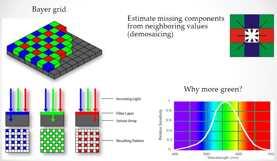
Fig:Bayer Grid
Source:Steve Seitz
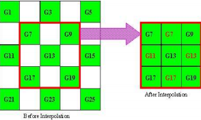
Fig:Color Interpolation
The missing arrays are interpolated by the average of the upper, lower, left and right pixel values of green
G8 = (G3+G7+G9+G13) / 4
Likewise red and blue missing arrays are also interpolated to give the exact picture
Circuit noise and processing of images
Thermal noise is observed in the resistive components present inside the pixels. This noise is present at all the times, i.e., it is present even in the complete darkness. So this noise in cameras is called darknoise.
Did you take any photo using DSLR?If yes,then you may have observed two click sounds coming from camera while taking an image.Have you ever thought about what these sounds signify?
When we click to capture photo, first the shutter of the DSLR will be closed and an image will be taken(with no light it just looks dark).This picture gives all the noises present in the circuits.This can be interpreted as first sound and that image can be called as DARK IMAGE which contains dark noise.
Now light gets focused on camera and an image will be captured as explained above.This represents the second sound.Now these two images are subtracted from one another assuming the noises produced by the circuits is the same in both the cases.
Some effects observed in photos
Before looking at some of the common effects that occur when we take a photograph, let’s look at an analogy which can be used to understand the concepts better.
Beer analogy
A pixel sensor can be compared to a beer glass.After getting the charge corresponding to the incident light,it gets transferred to a bucket which is responsible for the intensity of pixel.
Imagine a glass where you are trying to fill it with beer.How much we try to fill it,there will be some foam remaining at the top making it not 100% full.Also,how much ever you try to drain it,we cannot empty it completely.
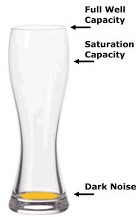
Beer Analogy
Source:image-sensors-blogspot
These can be explained in technical terms as
Full well capacity
The size of the glass → size of the bucket(CCD) which is responsible for pixel intensity
Saturation capacity
Maximum possible capacity that can be filled in glass → effective charge remaining in bucket
Dark Noise
Minimum amount of beer that’s unavoidable → represents noise effects which is unavoidable.
Dynamic range
It is the ratio of maximum capacity possible to the minimum capacity(noise) which is unavoidable.
In other words, it is the difference between the darkest and lightest tones in an image, generally pure black and pure white.
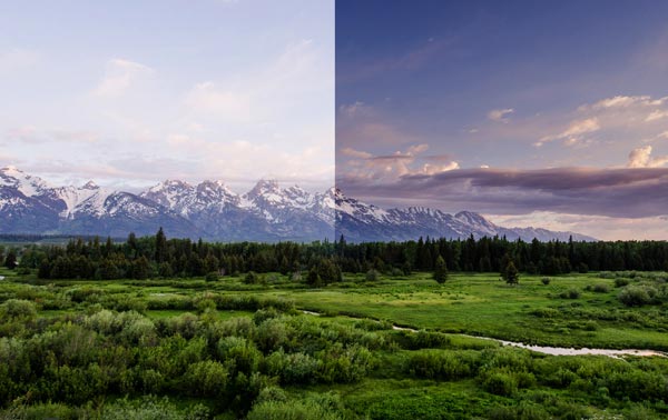
Fig:Effect of Dynamic Range
Source:adorama.com
Concept of blooming
From the image, if you keenly observe the area with light,it is not so clearly distinguishable.This can be understood in the following way

Fig:Blooming explained
Source:camerarepair.org
The pixel sensor that corresponds to this location gets saturated easily as it is exposed to high intensity.The bucket gets filled and the excess electrons that accumulate here are spilled and will be occupied by the neighbouring buckets thus raising their level which implies high intensity when processed.
Thus,the surroundings present at light source gets saturated due to the overflow of bucket which is called as blooming.
How to avoid blooming?
To avoid blooming we need to know some terms in camera
Aperture
The size of lens which allows the light to flow inside and excite electrons is aperture.
Measured by f-stop/f-number.
Higher f-stop → less aperture → allowing less light
Smaller f-stop → More aperture → allowing more light
f/1 → Largest opening aperture. f/180 → Smallest opening aperture
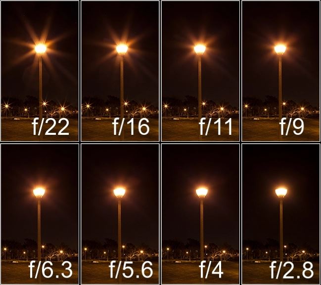
Fig:Aperture effect explained
Source:slrlounge.com
Shutter speed
It is the speed with which the image is being taken i.e the speed with which light is captured and image is formed. Or the time for which light is allowed to fall on lens
More shutter speed → Allowing less amount of light(as ON for less time)
Less shutter speed → Allowing more amount of light(as ON for more time)
1/2 → low shutter speed
1/1000 → High shutter speed
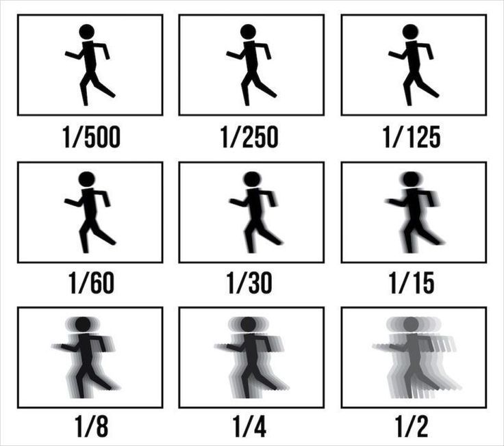
Fig:Shutter speed explained
ISO
It represents the sensitivity of camera towards light. Higher the number, higher the sensitivity towards light and vice versa. As ISO number increases, the brightness of photo increases. More ISO also adds noise.
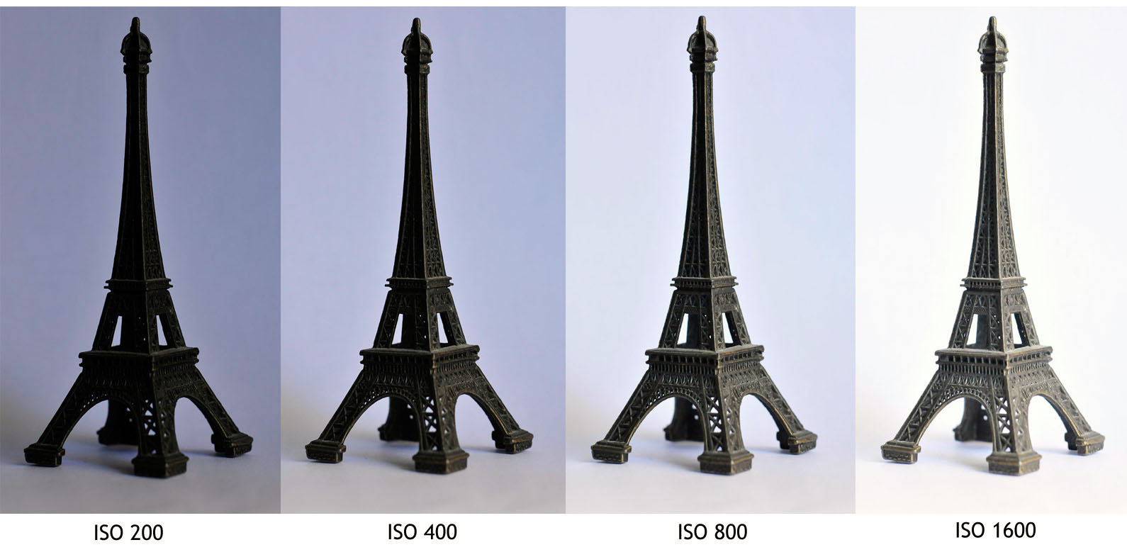
Fig:ISO explained
Source:strevdev.wordpress
After getting this analog value,this is transferred using buses to ADC which converts it to an equivalent digital value which can be viewed on screen.
Analog Digital Converter
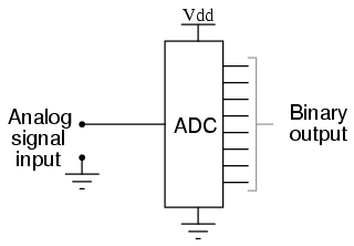
Fig:Analog to Digital Converter
Fun time
What features do you think are better to take a photo
- Day time, a vehicle going at a high speed?
- Night time, a building?
- To avoid blooming of images, what will you consider?